1 Introduction
Diamond wire cutting technology is also known as fixed abrasive cutting technology. It is the use of electroplating or resin bonding method of the diamond abrasive on the surface of the steel wire, the diamond wire directly on the surface of the silicon rod or silicon ingot grinding, to achieve the cutting effect. Diamond wire cutting has the advantages of fast cutting speed, high cutting precision and low material loss.
At present, the single-crystal market has completely accepted the diamond wire cutting wafers, but it has also encountered in the process of advancement, in which whitening is the most common problem. In view of this, this article focuses on how to prevent the problems of diamond white wire cutting single crystal silicon.
The diamond wire cutting single crystal silicon wafer cleaning process is to remove the silicon wafer that has been cut by the wire saw machine tool from the resin plate, and after the strip is removed, the silicon wafer is cleaned. Cleaning equipment is mainly pre-cleaning machine (degumming machine) and cleaning machine. The main cleaning process of the pre-washing machine is: feeding-spraying-spraying-ultrasonic cleaning-ungluing-rinsing-rinsing-feeding. The main cleaning process of the washing machine is: feeding - pure water rinsing - pure water rinsing - alkaline washing - alkaline washing - pure water rinsing - pure water rinsing - pre-dehydration (slow lifting) - drying - cutting.
2. The principle of single crystal wool
Single-crystal silicon wafers are used to prepare suede by the anisotropic etching of monocrystalline silicon wafers using alkali liquor. The reaction principle is as follows chemical reaction equation
Si+2NaOH+H2O=Na2SiO3+2H2
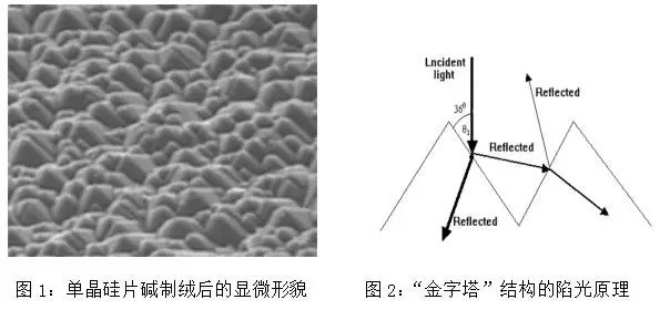
In essence, the suede formation process is: the etching rate of different crystal faces is different for NaOH solution, and the etching speed of the (100) surface is more than ten times larger than the (111) surface, so the single crystal silicon wafer with (100) crystal orientation After anisotropic etching, a large number of tetrahedral pyramids with a (111) surface are finally formed on the surface, ie, a “pyramid†structure (see FIG. 1 ). After this structure is formed, when the light is incident on the slope of the pyramid at a certain angle, the light will be reflected to the slope at another angle, forming a second or more absorption, thereby reducing the reflectivity of the surface of the wafer, ie, the trapping effect (as shown in FIG. 2). The better the size and uniformity of the “pyramid†structure, the more obvious the trapping effect and the lower the surface emissivity of the silicon wafer.

3 single crystal cashmere whitening analysis
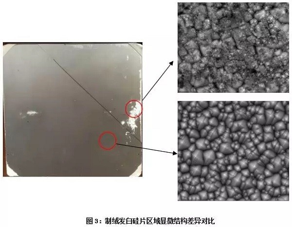
Scanning electron microscopy was performed on the whitish silicon wafers. It was found that the napped pyramids had almost no pyramidal microstructure and that the surface appeared to have a “waxy†residue on the surface and that the same silicon was present. The formation of a suede pyramid structure with no whitish regions is better (Figure 3). If there is residue in the local area of ​​the surface of the single crystal silicon wafer, there will be a residual area “pyramid†on the surface of the silicon wafer. The size and uniformity of the structure will be less than that of the normal area, resulting in a lower reflectivity of the textured surface than the normal area. High, high-reflectivity areas visually appear whitish compared to normal areas. From the distribution of the whitish region, it can be seen that it is not a regular or regular shape that appears over a large area, but only appears in a local area. It should be that the local contaminants on the surface of the silicon wafer have not been cleaned, or the silicon surface The situation was caused by secondary pollution.

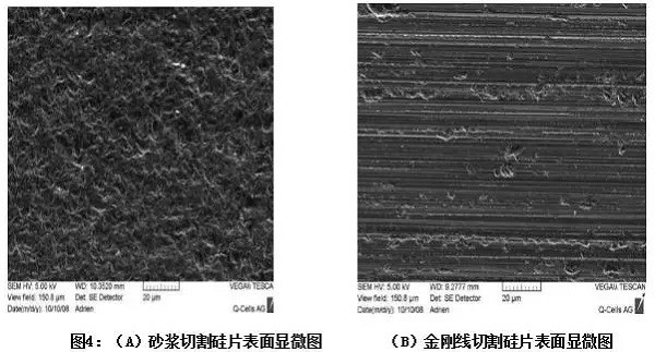
Diamond wire cutting silicon surface is smoother and less damaging (Fig. 4). Compared to mortar silicon wafers, the reaction rate of lye and diamond wire cutting the surface of silicon wafers is higher than that of mortar cutting single crystal silicon wafers. Slow, so the effect of surface residue on the texturing effect is even more pronounced.

4. Diamond wire cutting surface of the main residual source of silicon
(1) Coolant: The main components of diamond wire cutting coolant are surfactants, dispersants, defoamers, and water. Excellent cutting fluid has good suspension, dispersion and easy cleaning. Surfactants are generally able to have good hydrophilicity and are easier to wash off during wafer cleaning. The continuous stirring and circulation of these auxiliaries in the water will generate a large amount of bubbles, resulting in a drop in the flow of the cooling liquid, an effect on the cooling performance, and even a problem of foam overflow and even foam overflow, which will seriously affect the use. Therefore, the coolant is usually used with defoamers. The traditional defoamers of silicones and polyethers to ensure defoaming performance, defoamers are usually poor in hydrophilicity, and the solvent is demulsified and precipitated in water, so it is easy to adsorb and remain on the surface of silicon wafers in the subsequent cleaning process. There is a problem with flock white spots.
And can not be a good compatibility with the main components of the coolant, it must be made into two components, the use of the dilution of the main component and defoamer were diluted in water, respectively, in the use of the process according to the need to add foam, can not be quantitative control The use of anti-foaming agents and the amount of supplements, it is easy to make excessive use of defoamers, resulting in increased surface residue on the silicon wafer, the operation is also more inconvenient, but because of the main raw material and defoamer raw material prices are relatively low, so Most of the domestic coolants use this formula system; the other coolant adopts a new defoamer, which can be well-matched with the main components, and does not require supplementation. It can effectively control the amount of its use, and can effectively prevent overdosing. It is very easy to use and operate. With proper cleaning process, the residue can be controlled to a very low level. Japan and a few domestic manufacturers use this formula system, but due to the high raw material cost, the price advantage is not obvious. .
(2) Glue and resin version: At the later stage of the diamond wire cutting process, the silicon wafers near the inlet end have been cut through beforehand, and the outlet end silicon wafer has not yet been cut through. The diamond wire that has been cut in advance has already been cut into the adhesive layer and the resin plate. Because the silicon stick glue and the resin board are all epoxy resin products, the softening point is basically between 55-95°C. If the softening point of the adhesive layer or the resin plate is low, it is easy to cause heat to change during the cutting process. Soft-melting, adheres to the surface of steel wire and silicon wafers, causing the cutting ability of the diamond wire to decrease, or the silicon wafer is contaminated with resin. Once attached, it is difficult to wash away. Such contamination often occurs at the cutting surface of the silicon wafer. Near the edge.
(3) Silica fume: A large amount of silicon powder will be produced during diamond cutting. As the cutting progresses, the content of fine powder in the coolant will be higher and higher, and when the amount of fine powder is large enough, it will adhere to the silicon. The surface of the sheet, and the grain size and particle size of the silicon powder produced by wire cutting, make it easier to adsorb on the surface of the silicon wafer, making it difficult to clean. Therefore, when the silicon block is cut, the amount and quality of the cooling liquid must be guaranteed, and the content of the fine powder in the cooling liquid should be reduced.
(4) Cleaning agent: Most diamond wire cutting manufacturers currently use mortar for cutting at the same time. Most of them still follow the pre-rinsing, cleaning processes and cleaning agents used for mortar cutting, and the single diamond wire cutting technology from the cutting mechanism, the supporting wire, There is a big difference between the cooling fluid and the mortar cutting, so the corresponding cleaning process, the amount of the cleaning agent, and the formula should be adjusted accordingly for the diamond wire cutting. The cleaning agent is an important aspect. The surfactants, alkalinity, etc. in the original cleaning agent formulation may not be suitable for cleaning diamond wire-cut wafers, and should be directed to the surface conditions of the diamond wire silicon wafers, components in the cooling fluid, and In the case of surface residues, targeted cleaning agents were developed and the cleaning process was matched with them. The defoamer composition as described above is an ingredient not required for mortar cutting.
(5) Water: Diamond wire cutting, pre-rinsing, and wash overflowing water may adsorb to the surface of silicon wafers if they contain impurities.
5.Reducing the occurrence of whitening problems in diamond wire cut single crystal silicon wafers
(1) The use of a good dispersion of coolant requires the use of a low-residual defoamer in the coolant to reduce the residual of coolant components on the surface of the silicon wafer;
(2) Use suitable glue and resin plates to reduce the contamination of silicon wafers;
(3) The coolant is diluted with pure water to ensure that there is no residue that is easily retained in the water used;
(4) For the surface of silicon wafers cut by diamond wire, use cleaners with better activity and cleaning effect;
(5) The diamond online coolant recovery system is used to reduce the content of silicon powder in the cutting process, so as to effectively control the residual silicon powder on the surface of the silicon wafer. At the same time, it can also improve the water temperature, flow rate and time in the pre-rinsing to ensure silicon. Flush in time
(6) Once the silicon wafer is placed on the cleaning table, it must be processed immediately to keep the wafer wet throughout the cleaning process.
(7) The silicon wafer keeps the surface wet during degumming and cannot dry naturally.
(8) During the cleaning process, the silicon wafer minimizes the exposure time in the air, so as to prevent the wafer surface from generating flower patches.
(9) The cleaning staff shall not directly touch the surface of the wafer during the entire cleaning process, and must wear rubber gloves to avoid fingerprints.
(10) The use of hydrogen peroxide H2O2 + alkali NaOH at the cell end in a volumetric ratio of 1:26 (3% NaOH solution) for the cleaning process can effectively reduce the occurrence of white spots. The principle is similar to the SC1 cleaning liquid (commonly known as No. 1 liquid) of semiconductor silicon wafers. The main mechanism of action is that an oxide film is formed on the surface of the silicon wafer due to the oxidation of H2O2. The oxide film is again corroded by NaOH. Immediately after the corrosion, oxidation, oxidation, and corrosion occur repeatedly, so particles attached to the surface of the silicon wafer (such as silicon powder, Resin, metal, etc. also fall into the cleaning solution with the etching layer; due to the oxidation of H2O2, the organic matter on the wafer surface is decomposed into CO2 and H2O and removed. This cleaning process currently has silicon wafer manufacturers using this process to handle the diamond wire cut single crystal silicon wafers. The silicon wafers have been used in domestic and Taiwan and other battery manufacturers in batches without complaints of woollen whitening problems. There are also battery manufacturers also use a similar pre-washing process, but also effectively control the appearance of cashmere. It can be seen that the cleaning process is added to the silicon wafer cleaning process to remove the silicon wafer residue and effectively solve the problem of battering and whitening of the battery end.
6. Summary
At present, diamond wire cutting has become the main processing technology in the field of single crystal cutting, but the problem of bast and whitening has been plaguing silicon wafers and battery manufacturers during the process of advancement, resulting in some contradictions between the battery manufacturers and the silicon wafers cut by diamond wires. . Through the comparison analysis of the white areas, it was found that the velvet and whitening was mainly caused by the presence of residues on the surface of the silicon wafer. In order to better prevent the whitening problem of the silicon wafer at the end of the cell, this paper analyzes possible sources of possible contamination of the silicon wafer surface, as well as suggestions and measures for improvement during production. The cause analysis and improvement can be carried out according to the number, area, shape, etc. of the occurrence of leukoplakia. It is particularly recommended to use hydrogen peroxide + alkali cleaning and cleaning process, and successful experience has proved that it can effectively prevent the problem of diamond white silicon wool cutting and whitening, for the majority of industry insiders and manufacturers reference.
Round Holes Perforated Metal Sheet
Perforated metal Sheet is also called perforated plate or punched metal plate.Perforated Metal Sheet can be offered with various hole shape, and we can recommend suitable hole size according to your request on hole shape and open area.
Diameter: 0.5 -100 mm
Sheet Thickness: From 0,3 mm to 10mm
Size: 1000mm*2000mm 1220*2440mm 1500*3000mm Customized size can be available.
Material :Carbon steel, Aluminum, Stainless steel ,Galvanized steel etc.
Packaging: Wooden crates or pallets
Productivity: 200 square meters per day
MOQ:5pcs or negotiated
Applications:
Architectural screen
Filters
Guard grills
Heavy mining machinery
Metal ceilings
Agricultural separation
Product Advantage:
1. Easy to process and shape. 2. Easy to install.
3. Can be painted or polished. 4. Attractive appearance.
5. Plates of various thicknesses. 6. Multiple choice of aperture and arrangement.
7. Good sound absorption effect.
Perforated Metal,Perforated Sheet Metal,Stainless Steel Perforated Metal,Galvanized Steel Expanded Metal
HEBEI KAYI BUILDING MATERIAL TECHNOLOGY CO.,LTD , https://www.kayigrating.com